| CPC H01L 29/0847 (2013.01) [H01L 21/76846 (2013.01); H01L 23/528 (2013.01); H01L 23/53209 (2013.01); H01L 29/0653 (2013.01); H01L 29/41791 (2013.01); H01L 29/4236 (2013.01); H01L 2924/13067 (2013.01)] | 18 Claims |
|
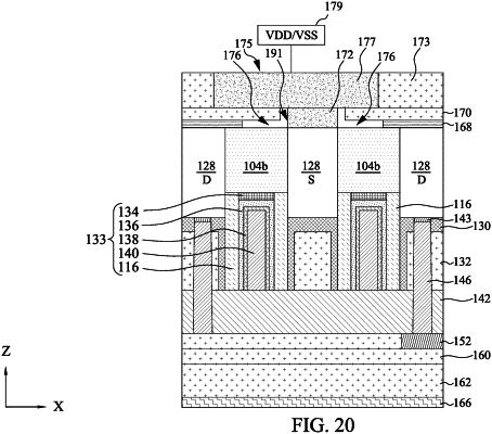
1. A semiconductor device structure, comprising:
a substrate having a front side and a back side opposing the front side;
a gate stack disposed on the front side of the substrate;
a first source/drain feature and a second source/drain feature disposed in opposing sides of the gate stack, each first source/drain feature and second source/drain feature comprises a first side and a second side;
a contact etch stop layer (CESL) in contact with the first side of the first source/drain feature; and
a conductive feature in contact with the second side of the first source/drain feature,
wherein a portion of the back side of the substrate and the conductive feature are exposed to an air gap.
|