| CPC H01L 29/0847 (2013.01) [H01L 21/0217 (2013.01); H01L 21/02636 (2013.01); H01L 21/26513 (2013.01); H01L 21/26586 (2013.01); H01L 21/30604 (2013.01); H01L 29/0649 (2013.01); H01L 29/167 (2013.01); H01L 29/36 (2013.01); H01L 29/6656 (2013.01); H01L 29/66575 (2013.01); H01L 29/66636 (2013.01); H01L 29/66795 (2013.01); H01L 29/7833 (2013.01); H01L 29/7851 (2013.01); H01L 21/02529 (2013.01); H01L 21/02532 (2013.01); H01L 21/266 (2013.01); H01L 29/165 (2013.01); H01L 29/66545 (2013.01); H01L 29/7848 (2013.01)] | 20 Claims |

|
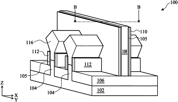
1. A semiconductor device, comprising:
a substrate;
an isolation structure over the substrate;
a fin over the substrate and the isolation structure;
a gate structure engaging a first portion of the fin;
first sidewall spacers over sidewalls of the gate structure and over a second portion of the fin;
source/drain (S/D) features adjacent to the first sidewall spacers; and
second sidewall spacers over the isolation structure and over sidewalls of a portion of the S/D features, wherein the second sidewall spacers include silicon oxide, silicon nitride, or silicon oxynitride, wherein the second sidewall spacers and the second portion of the fin include a same dopant, wherein the dopant includes phosphorus.
|