| CPC H01L 29/0657 (2013.01) [H01L 27/088 (2013.01); H01L 29/42392 (2013.01); H01L 29/78696 (2013.01)] | 20 Claims |

|
1. A method for manufacturing a semiconductor device comprising:
forming a mask layer on a substrate;
forming spacers spaced apart from each other on the mask layer;
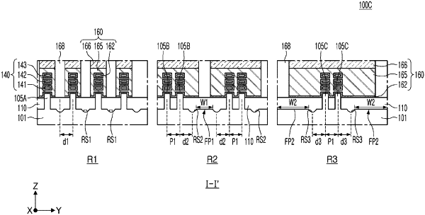
forming mask patterns by etching the mask layer using the spacers as an etching mask, the mask patterns including fin mask patterns, guard mask patterns, and dummy mask patterns;
removing the dummy mask patterns;
forming fin patterns by etching the substrate using the fin mask patterns and the guard mask patterns as etching masks, the fin patterns including active fin patterns and guard fin patterns;
forming recess portions on the substrate by removing the guard fin patterns;
forming a device isolation layer on the substrate, upper portions of the active fin patterns protruding from an upper surface of the device isolation layer; and
forming gate structures on the device isolation layer, the gate structures intersecting the active fin patterns and extending in a second direction.
|