| CPC H01L 29/0653 (2013.01) [H01L 29/42376 (2013.01); H01L 29/7816 (2013.01)] | 19 Claims |
|
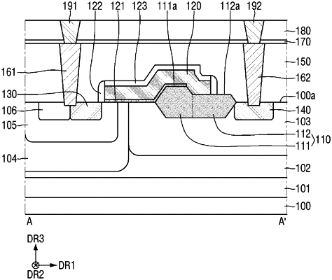
1. A semiconductor device comprising:
a substrate;
a gate electrode disposed on an upper surface of the substrate;
a source region disposed on a first side of the gate electrode;
a drain region disposed on a second side of the gate electrode opposite to the first side of the gate electrode in a horizontal direction;
an insulating structure at least partially buried inside the substrate, wherein the insulating structure comprises a first portion disposed between the substrate and the gate electrode, and a second portion in contact with the drain region;
a gate insulating layer disposed between the upper surface of the substrate and the gate electrode; and
a gate spacer disposed on each of the first side and the second side of the gate electrode,
wherein an uppermost surface of the second portion of the insulating structure is lower than an uppermost surface of the first portion of the insulating structure,
wherein at least a part of the gate electrode is disposed on the uppermost surface of the second portion of the insulating structure, and
wherein the gate spacer disposed on the second side of the gate electrode is in contact with the uppermost surface of the second portion of the insulating structure.
|