| CPC H01L 28/82 (2013.01) [H01L 27/0805 (2013.01); H01L 28/91 (2013.01); H10B 12/01 (2023.02); H10B 12/02 (2023.02); H10B 12/315 (2023.02)] | 7 Claims |
|
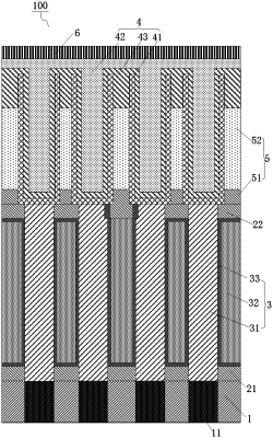
1. A semiconductor structure, comprising:
a substrate;
a first capacitor located on the substrate, wherein the first capacitor comprises a first bottom electrode, a first dielectric layer and a first top electrode, the first bottom electrode is of a columnar structure, the first dielectric layer covers the first bottom electrode, and the first top electrode is located on one surface of the first dielectric layer away from the first bottom electrode; and
a second capacitor, located above the first capacitor, wherein the second capacitor comprises a second bottom electrode being of a concave structure and electrically connected with the first bottom electrode, a second dielectric layer filling and covering the second bottom electrode, and a second top electrode;
wherein the second dielectric layer is located between the second bottom electrode and the second top electrode, and the second dielectric layer is further located between the second bottom electrodes of adjacent second capacitors,
wherein the semiconductor structure further comprises a first supporting layer, a second supporting layer and a third supporting layer, the first supporting layer is located at a periphery of a bottom of the first bottom electrode, and the second supporting layer is located at a periphery of a top of the first bottom electrode, the third supporting layer is located at a periphery of a bottom of the second bottom electrode, and part of the third supporting layer is disposed in the second supporting layer such that a line extending parallel to a top surface of the substrate intersects both the part of the third supporting layer and the second supporting layer, and
wherein the second dielectric layer fully fills a partial space between the second bottom electrodes of the adjacent second capacitors, and the partial space is away from the third supporting layer.
|