| CPC H01L 27/156 (2013.01) [H01L 33/24 (2013.01); H01L 33/38 (2013.01); H01L 33/44 (2013.01); H01L 2933/0016 (2013.01)] | 18 Claims |
|
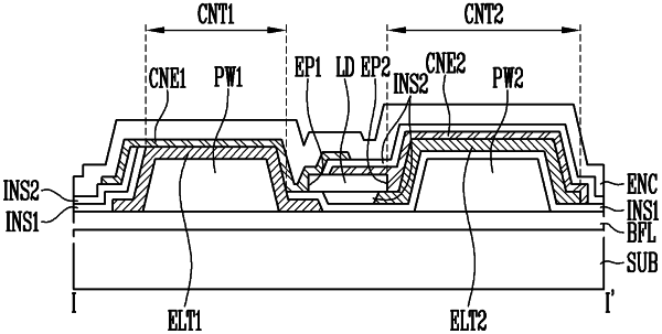
1. A light emitting device comprising:
a first electrode having a first lower surface disposed on a substrate;
a first insulating layer having a second lower surface disposed on the substrate and coplanar with the first lower surface at a first portion of the first insulating layer, the second lower surface overlapping at least a part of the first electrode at a second portion of the first insulating layer;
a second electrode disposed on the first insulating layer and spaced apart from the first electrode; and
at least one light emitting diode disposed on the first insulating layer and electrically connected between the first electrode and the second electrode, wherein
the first electrode and the second electrode are disposed on different layers on the substrate,
the first insulating layer is disposed between the first electrode and the second electrode,
the first electrode and the second electrode are spaced apart from each other so as not to overlap each other in a plan view,
the light emitting device further comprises a display element layer including the first electrode, the second electrode, and the least one light emitting diode, and a circuit element layer disposed between the display element layer and the substrate, and
the circuit element layer comprises: a first circuit element or a first power line electrically connected to the first electrode and including a part overlapping the second electrode; and a second circuit element or a second power line electrically connected to the second electrode and including a part overlapping the first electrode.
|