| CPC H01L 27/14643 (2013.01) [H01L 27/14603 (2013.01); H04N 25/70 (2023.01)] | 20 Claims |

|
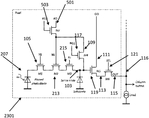
1. Imaging device comprising:
a substrate;
a pinned photodiode formed on the substrate, wherein the pinned photodiode generates a charge that is representative of incident radiation;
a first circuit defining a first path for measuring the charge and configured to non-destructively produce a first signal representative of the charge generated in the pinned photodiode, wherein the first circuit comprises:
a sense gate electrode formed on the substrate to capacitively couple the substrate to the charge; and
a measurement circuit configured to measure a voltage change of the sense gate;
a second circuit defining a second path for measuring the charge and configured to destructively produce a second signal representative of the charge; and
a readout circuit common to the first path and to the second path and comprising a source follower,
wherein the first path has a first conversion gain, the second path has a second conversion gain, and the first conversion gain differs from the second conversion gain.
|