| CPC H01L 27/1464 (2013.01) [H01L 27/14605 (2013.01); H01L 27/14614 (2013.01); H01L 27/14623 (2013.01); H01L 27/14638 (2013.01); H01L 27/14643 (2013.01); H01L 27/14683 (2013.01); H01L 27/14689 (2013.01); H01L 27/14818 (2013.01)] | 15 Claims |

|
1. A semiconductor device, comprising:
a semiconductor substrate; and
a transfer transistor that is part of a pixel circuit, the transfer transistor being disposed at a first side of the semiconductor substrate, the transfer transistor including a source region, a drain region and a gate electrode, the transfer transistor being configured to transfer charge from a photoelectric conversion element to a charge holding section,
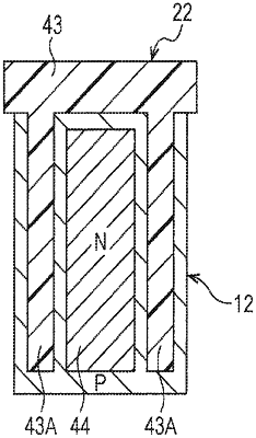
the gate electrode of the transfer transistor including a connecting portion, a first trench gate section and a second trench gate section in a cross-section view, wherein
the connecting portion is disposed on a first surface of the semiconductor substrate and is connected to the first trench gate section and the second trench gate section,
the first trench gate section and the second trench gate section are disposed in a depth direction of the semiconductor substrate,
a portion of the semiconductor substrate is disposed between the first trench gate section and the second trench gate section, and
one of the source region or the drain region of the transfer transistor is disposed between the first trench gate section and the second trench gate section and underneath the connecting portion.
|