| CPC H01L 27/14636 (2013.01) [H01L 27/14601 (2013.01); H01L 27/14634 (2013.01); H01L 27/1464 (2013.01); H01L 27/14645 (2013.01); H01L 27/14685 (2013.01); H01L 27/14687 (2013.01); H01L 27/1469 (2013.01); H01L 31/09 (2013.01); H01L 27/14621 (2013.01)] | 62 Claims |
|
1. A device comprising:
a first substrate;
a second substrate which overlaps the first substrate;
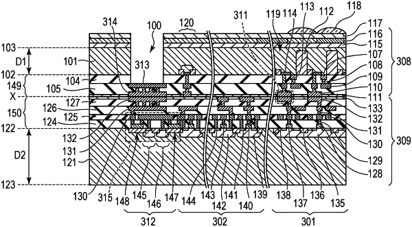
a first structure which is between the first substrate and the second substrate, the first structure including a first film of a dielectric material and a first portion of a conductive material, the first portion being in a groove of the first film; and
a second structure which is between the first structure and the second substrate, the second structure including a second film of a dielectric material and a second portion of a conductive material, the second portion being in a groove of the second film,
wherein a first face of the first film is bonded to a second face of the second film, and the first portion is bonded to the second portion, and
wherein the first portion includes a first conductive portion of a first conductive material, the first portion includes a first conductive film of a second conductive material other than the first conductive material,
the first film includes a diffusion preventing film configured to prevent a diffusion of a material from the first portion or the second portion, and
the first conductive film contacts the first film.
|