US 12,068,346 B2
Solid-state image sensor and electronic device
Shinji Miyazawa, Kanagawa (JP); and Yutaka Ooka, Kanagawa (JP)
Assigned to Sony Group Corporation, Tokyo (JP)
Filed by SONY GROUP CORPORATION, Tokyo (JP)
Filed on Dec. 27, 2022, as Appl. No. 18/146,829.
Application 18/146,829 is a continuation of application No. 16/874,442, filed on May 14, 2020, granted, now 11,581,346.
Application 16/874,442 is a continuation of application No. 15/912,186, filed on Mar. 5, 2018, granted, now 10,756,130, issued on Aug. 25, 2020.
Application 15/912,186 is a continuation of application No. 15/691,529, filed on Aug. 30, 2017, granted, now 9,929,197, issued on Mar. 27, 2018.
Application 15/691,529 is a continuation of application No. 15/476,554, filed on Mar. 31, 2017, granted, now 9,812,479, issued on Nov. 7, 2017.
Application 15/476,554 is a continuation of application No. 15/015,984, filed on Feb. 4, 2016, granted, now 10,032,816, issued on Jul. 24, 2018.
Application 15/015,984 is a continuation of application No. 14/011,193, filed on Aug. 27, 2013, granted, now 9,257,474, issued on Feb. 9, 2016.
Claims priority of application No. 2012-203069 (JP), filed on Sep. 14, 2012.
Prior Publication US 2023/0134510 A1, May 4, 2023
Int. Cl. H01L 27/146 (2006.01)
CPC H01L 27/14618 (2013.01) [H01L 27/14621 (2013.01); H01L 27/14623 (2013.01); H01L 27/14627 (2013.01); H01L 27/14636 (2013.01); H01L 27/14645 (2013.01); H01L 27/14685 (2013.01)] 20 Claims
OG exemplary drawing
 
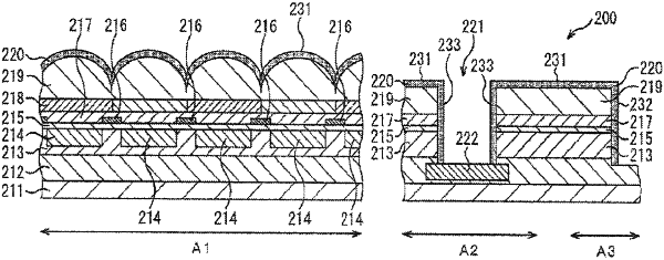
1. A solid-state imaging device, comprising:
a substrate including:
a plurality of photodiodes;
a first side as a light-incident side; and
a second side opposite to the first side; and
a protection film including:
a side wall part extending in a direction towards the second side of the substrate; and
a ceiling part,
wherein the ceiling part covers a region where the plurality of photodiodes are arranged over the substrate,
wherein the side wall part covers a side surface of a color filter layer and a side surface of the substrate,
wherein the protection film is further formed along an inner side wall of an opening for wiring to an electrode pad of the solid-state imaging device, and
wherein the electrode pad is formed below the plurality of photodiodes.