| CPC H01L 27/14618 (2013.01) [H01L 27/14683 (2013.01); H01L 31/0203 (2013.01)] | 19 Claims |
|
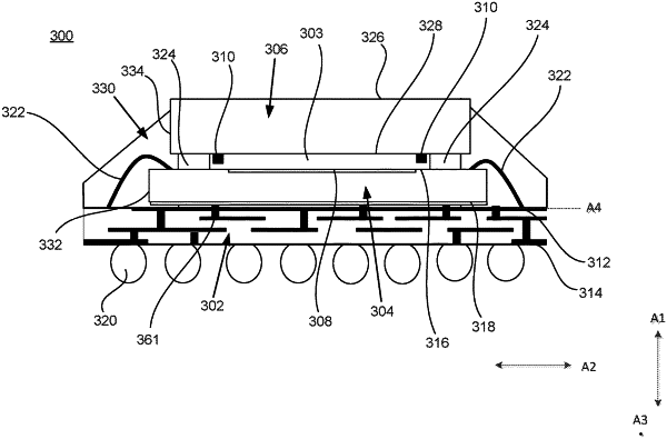
1. A sensor package comprising:
a substrate including an image sensor die, the image sensor die having an active area configured to receive an incoming optical signal;
a transparent layer including a first surface and a second surface, the first surface positioned at an edge of the sensor package and the second surface facing the image sensor die;
at least one dam member that couples a first portion of the second surface of the transparent layer to the image sensor die; and
a light blocking layer that contacts a second portion of the second surface of the transparent layer and that surrounds the active area of the image sensor die, the second portion being adjacent to the first portion, the light blocking layer not contacting the first portion.
|