| CPC H01L 27/14614 (2013.01) [H01L 27/1463 (2013.01); H04N 25/75 (2023.01)] | 20 Claims |
|
1. An image sensing device comprising:
a plurality of unit pixel regions arranged in a first direction and a second direction perpendicular to the first direction in a substrate;
a first device isolation region supported by the substrate and structured to isolate the plurality of unit pixel regions from each other;
a plurality of photoelectric conversion regions supported by the substrate and formed in the plurality of unit pixel regions in the substrate to form a plurality of imaging pixels structured to generate photocharges by performing photoelectric conversion of incident light;
a plurality of second device isolation regions supported by the substrate to define active regions of the plurality of imaging pixels;
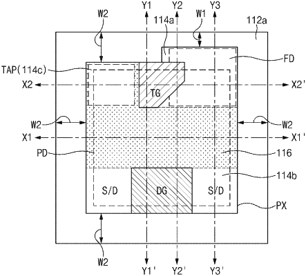
a plurality of floating diffusion regions formed in a first active region to store the photocharges generated by the photoelectric conversion regions; and
a plurality of transfer gates structured to transmit the photocharges generated by the photoelectric conversion regions to the plurality of the floating diffusion region,
wherein each of the floating diffusion regions is located contiguous to only one of two sides of a corresponding transfer gate in the first direction and contiguous to two sides of the corresponding transfer gate in the second direction.
|