| CPC H01L 27/14612 (2013.01) [H01L 31/02019 (2013.01); H01L 31/101 (2013.01); B60R 11/04 (2013.01)] | 15 Claims |

|
1. A photoelectric conversion device having a plurality of pixels, each of the plurality of pixels comprising:
a semiconductor substrate;
a photoelectric conversion unit disposed inside the semiconductor substrate;
a floating diffusion to which a signal carrier generated by the photoelectric conversion unit is transferred;
an amplification transistor configured to output a signal from the photoelectric conversion unit to an output line;
a selection transistor configured to connect the amplification transistor to the output line;
a reset transistor configured to be connected to the floating diffusion;
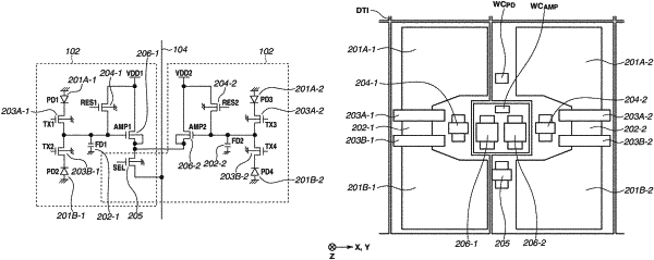
an insulating isolation portion, disposed between the amplification transistor and the photoelectric conversion unit and between the amplification transistor and the selection transistor to surround the amplification transistor in a plan view, configured to penetrate through the semiconductor substrate;
a first well in which the amplification transistor is disposed;
a second well in which the reset transistor and the selection transistor are disposed; and
a well contact which is disposed in the first well,
wherein a source and a drain of the amplification transistor are a first conductivity type semiconductor,
wherein the well contact is a second conductivity type semiconductor which is different from the first conductivity type semiconductor,
wherein the well contact is electrically connected to the first well, and
wherein the insulating isolation portion is disposed between the amplification transistor, and the reset transistor and the select transistor,
wherein a plurality of the amplification transistors is disposed in a region surrounded by the insulating isolation portion, and
wherein, in the plurality of amplification transistors, a voltage applied to a gate of the amplification transistor that does not perform readout is lower than a voltage applied to a gate of the amplification transistor that performs readout.
|