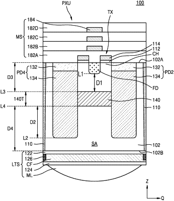
| CPC H01L 27/1461 (2013.01) [H01L 27/14603 (2013.01); H01L 27/14621 (2013.01); H01L 27/14627 (2013.01); H01L 27/1463 (2013.01); H01L 27/1464 (2013.01); H01L 27/14641 (2013.01); H01L 27/14645 (2013.01)] | 20 Claims |

|
1. An image sensor comprising:
a substrate having a sensing area;
a floating diffusion region arranged in the sensing area;
a plurality of photodiodes arranged around the floating diffusion region in the sensing area, wherein each of the plurality of photodiodes includes a first semiconductor region and a second semiconductor region; and
an inter-pixel overflow (IPO) barrier in contact with each of the plurality of photodiodes, wherein the IPO barrier includes a third semiconductor region in contact with the second semiconductor region of each of the plurality of photodiodes, the third semiconductor region having a same conductivity type as the second semiconductor region of each of the plurality of photodiodes, and the IPO barrier overlapping the floating diffusion region in a vertical direction at a position vertically spaced apart from the floating diffusion region within the sensing area.
|