| CPC H01L 27/1288 (2013.01) [G02F 1/136227 (2013.01); H01L 25/167 (2013.01); H01L 27/124 (2013.01); H01L 27/1248 (2013.01)] | 19 Claims |
|
1. A display device, comprising:
a substrate that includes a display area and a non-display area NDA outside the display area;
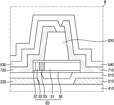
a first conductive layer disposed on the substrate, the first conductive layer including a first source/drain electrode of a transistor;
a passivation layer disposed on the first conductive layer and exposing at least a part of the first conductive layer in the display area;
a second conductive layer disposed on the passivation layer and covering an upper surface of the passivation layer in the display area;
a via layer disposed on the second conductive layer;
a third conductive layer including a first electrode, a second electrode, and a connection pattern spaced apart from each other on the via layer; and
a light emitting element having ends that are disposed on the first electrode and the second electrode, respectively, wherein
a first end of the light emitting element is electrically connected to the first electrode,
a second end of the light emitting element is electrically connected to the second electrode, and
the connection pattern electrically connects the first conductive layer and the second conductive layer through a first contact hole penetrating the via layer.
|