| CPC H01L 27/1255 (2013.01) [G09G 3/3233 (2013.01); H01L 27/1225 (2013.01); H01L 29/7869 (2013.01); H01L 29/78648 (2013.01); H10K 59/123 (2023.02)] | 9 Claims |
|
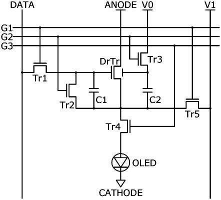
1. A light emitting device comprising a pixel, the pixel comprising:
a first transistor;
a second transistor:
a third transistor;
a fourth transistor;
a fifth transistor;
a sixth transistor;
a first capacitor; and
a light emitting element,
wherein,
one of a source and a drain of the first transistor is electrically connected to one of a source and a drain of the sixth transistor,
the other of the source and the drain of the first transistor is electrically connected to a first wiring,
a first gate of the first transistor is electrically connected to one of a source and a drain of the second transistor and to an electrode of the first capacitor,
a second gate of the first transistor is electrically connected to one of a source and a drain of the fourth transistor,
a gate of the second transistor is electrically connected a second wiring,
one of a source and a drain of the third transistor is electrically connected to the first gate of the first transistor,
a gate of the third transistor is electrically connected to a third wiring,
one of a source and a drain of the fourth transistor is electrically connected to a fourth wiring,
one of a source and a drain of the fifth transistor is electrically connected to the light emitting element,
the other of the source and the drain of the fifth transistor is electrically connected to a fifth wiring,
a gate of the sixth transistor is electrically connected to a sixth wiring,
the second transistor comprises an oxide semiconductor film, the oxide semiconductor film comprising a channel formation region,
the second wiring is different from the third wiring,
the third wiring is different from the sixth wiring,
the third wiring is configured to be supplied with a potential of a high level, and
the sixth wiring is configured to be supplied with a potential of a low level.
|