| CPC H01L 27/1255 (2013.01) [H01L 27/1288 (2013.01); H01L 27/1225 (2013.01); H01L 27/124 (2013.01)] | 12 Claims |

|
1. A display device comprising:
an active pattern disposed on a base substrate and including a metal oxide;
a gate electrode overlapping the active pattern;
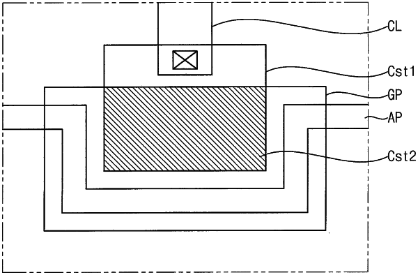
a first capacitor electrode including a conductive oxide;
a dummy semiconductor pattern between the first capacitor electrode and a planarized upper surface of the base substrate that faces the dummy semiconductor pattern and having a conductivity different from a conductivity of the first capacitor electrode, wherein an entire portion of a lower surface of the first capacitor electrode directly contacts an upper surface of the dummy semiconductor pattern without an intervening layer between the entire portion of the lower surface of the first capacitor electrode and the upper surface of the dummy semiconductor pattern;
an insulation layer disposed on the active pattern and the dummy semiconductor pattern, the insulation layer directly contacting a side surface of the active pattern and a side surface of the dummy semiconductor pattern; and
a second capacitor electrode on the first capacitor electrode, the first capacitor electrode being between the dummy semiconductor pattern and the second capacitor electrode,
wherein a thickness between a lower surface and the upper surface of the dummy semiconductor pattern is at least as great as a thickness between a lower surface and the upper surface of the active pattern.
|