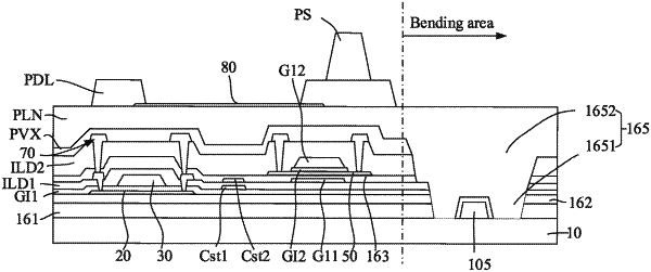
| CPC H01L 27/1251 (2013.01) [H01L 27/1225 (2013.01); H01L 29/78648 (2013.01); H10K 59/131 (2023.02); G09G 3/3233 (2013.01); G09G 2300/0426 (2013.01); H10K 59/351 (2023.02)] | 16 Claims |

|
1. A display substrate, comprising:
a base substrate;
a first semiconductor layer on the base substrate; and
a second semiconductor layer on a side of the first semiconductor layer away from the base substrate;
wherein the display substrate further comprises a plurality of thin film transistors on the base substrate, and the plurality of thin film transistors at least comprise a first transistor and a third transistor,
wherein each of the plurality of thin film transistors comprises an active layer, the active layer of the first transistor is located in the second semiconductor layer and contains an oxide semiconductor material, the active layer of the third transistor is located in the first semiconductor layer and contains a polysilicon semiconductor material;
wherein the first transistor comprises a first bottom gate electrode between the base substrate and the active layer of the first transistor, and a first top gate electrode on a side of the active layer of the first transistor away from the base substrate; and any two of an orthographic projection of the active layer of the first transistor on the base substrate, an orthographic projection of the first bottom gate electrode on the base substrate and an orthographic projection of the first top gate electrode on the base substrate at least partially overlap each other;
wherein the display substrate comprises a first conductive layer and a second conductive layer on the base substrate, the first conductive layer is located on the side of the first semiconductor layer away from the base substrate, and the second conductive layer is located between the first conductive layer and the second semiconductor layer;
wherein the third transistor comprises a gate electrode located in the first conductive layer, and a source electrode and a drain electrode located in the second conductive layer; and
wherein the first bottom gate electrode is located in the second conductive layer,
wherein the display substrate further comprises:
a second transistor comprising a second bottom gate electrode located between the base substrate and the active layer of the second transistor, and a second top gate electrode located on a side of the active layer of the second transistor away from the base substrate,
wherein any two of an orthographic projection of the active layer of the second transistor on the base substrate, an orthographic projection of the second bottom gate electrode on the base substrate and an orthographic projection of the second top gate electrode on the base substrate at least partially overlap each other, and
wherein the active layer of the second transistor is located in the second semiconductor layer and contains the oxide semiconductor material, and the second bottom gate electrode is located in the second conductive layer,
wherein the display substrate further comprises:
a first bottom gate structure located in the second conductive layer, wherein the first bottom gate structure comprises a first bottom gate body portion and a first bottom gate extension portion, an orthographic projection of the first bottom gate body portion on the base substrate at least partially overlaps the orthographic projection of the active layer of the first transistor on the base substrate, and the first bottom gate electrode comprises a portion of the first bottom gate body portion that overlaps the active layer of the first transistor; and/or
a second bottom gate structure located in the second conductive layer, wherein the second bottom gate structure comprises a second bottom gate body portion and a second bottom gate extension portion, an orthographic projection of the second bottom gate body portion on the base substrate at least partially overlaps the orthographic projection of the active layer of the second transistor on the base substrate, and the second bottom gate electrode comprises a portion of the second bottom gate body portion that overlaps the active layer of the second transistor,
wherein the display substrate further comprises a data line for transmitting a data signal, wherein the data line extends in a first direction on the base substrate, and at least one of the first bottom gate extension portion and the second bottom gate extension portion extends in the first direction; and wherein at least one of the active layer of the first transistor and the active layer of the second transistor extends in the first direction,
wherein the display substrate further comprises:
a third conductive layer on a side of the second semiconductor layer away from the base substrate; and
a first top gate structure located in the third conductive layer, wherein the first top gate structure extends in a second direction intersecting the first direction;
wherein the first top gate structure comprises a first widened portion, a size of the first widened portion in the first direction is greater than that of a remaining portion of the first top gate structure in the first direction; and
wherein an orthographic projection of the first widened portion on the base substrate at least partially overlaps the orthographic projection of the active layer of the first transistor on the base substrate, and the first top gate electrode comprises a portion of the first widened portion that overlaps the active layer of the first transistor.
|