US 12,068,331 B2
Flexible electronic device
Ti-Chung Chang, Miao-Li County (TW); Chih-Chieh Wang, Miao-Li County (TW); and Chien-Chih Chen, Miao-Li County (TW)
Assigned to INNOLUX CORPORATION, Miao-Li County (TW)
Filed by InnoLux Corporation, Miao-Li County (TW)
Filed on Apr. 21, 2023, as Appl. No. 18/304,483.
Application 18/304,483 is a continuation of application No. 17/109,263, filed on Dec. 2, 2020, granted, now 11,664,390.
Application 17/109,263 is a continuation of application No. 16/390,402, filed on Apr. 22, 2019, granted, now 10,886,307, issued on Jan. 5, 2021.
Claims priority of provisional application 62/673,212, filed on May 18, 2018.
Claims priority of application No. 201811196586.8 (CN), filed on Oct. 15, 2018.
Prior Publication US 2023/0261009 A1, Aug. 17, 2023
Int. Cl. H01L 27/12 (2006.01); G09F 9/30 (2006.01); H01L 23/498 (2006.01); H10K 77/10 (2023.01); H10K 102/00 (2023.01)
CPC H01L 27/1244 (2013.01) [H01L 23/4985 (2013.01); H01L 27/1218 (2013.01); H01L 27/1262 (2013.01); H10K 77/111 (2023.02); H10K 2102/311 (2023.02)] 9 Claims
OG exemplary drawing
 
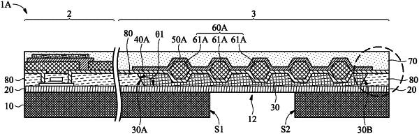
1. An electronic device having a peripheral area and a non-peripheral area adjacent to the peripheral area, comprising;
a flexible substrate;
a first conductive layer disposed on the flexible substrate and disposed in the peripheral area and the non-peripheral area;
an organic layer disposed in the non-peripheral area and on the first conductive layer;
a second conductive layer disposed on the first conductive layer; and
an organic structure disposed between and in direct contact with the first conductive layer and the second conductive layer in the peripheral area, wherein the organic layer and the organic structure are the same material layer.