| CPC H01L 27/1225 (2013.01) [H01L 29/247 (2013.01); H01L 29/66969 (2013.01); H01L 29/78618 (2013.01); H01L 29/78648 (2013.01); H01L 29/7869 (2013.01); H01L 29/78693 (2013.01); H01L 29/78696 (2013.01); G02F 1/133345 (2013.01); G02F 1/133528 (2013.01); G02F 1/134336 (2013.01); G02F 1/13439 (2013.01); G02F 1/136286 (2013.01); G02F 1/1368 (2013.01); G02F 2201/123 (2013.01); G09G 3/3674 (2013.01); G09G 2310/0286 (2013.01); H10K 59/1213 (2023.02)] | 19 Claims |
|
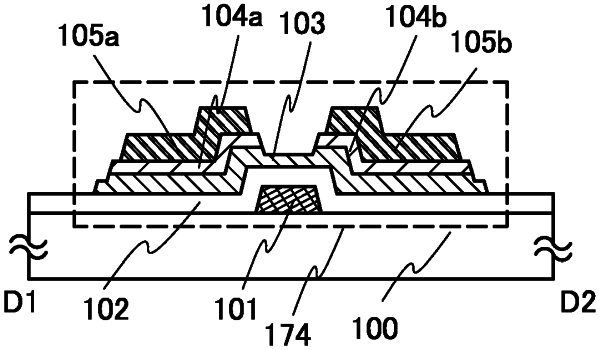
1. A semiconductor device comprising:
a gate electrode layer comprising copper;
a gate insulating layer over the gate electrode layer;
an oxide semiconductor layer over the gate insulating layer, the oxide semiconductor layer comprising a channel formation region of a transistor;
a first layer over the oxide semiconductor layer;
a second layer over the oxide semiconductor layer;
a first conductive layer electrically connected to the oxide semiconductor layer through the first layer; and
a second conductive layer electrically connected to the oxide semiconductor layer through the second layer,
wherein the first conductive layer is configured to function as one of a source electrode layer and a drain electrode layer,
wherein the second conductive layer is configured to function as the other of the source electrode layer and the drain electrode layer,
wherein, in a cross-sectional view in a channel length direction of the transistor:
an edge of the oxide semiconductor layer is provided in a first region beyond an edge of the first layer,
the edge of the first layer on the first region side is provided in a region beyond an edge of the first conductive layer, and
a film thickness of the oxide semiconductor layer in the first region is smaller than the film thickness of the oxide semiconductor layer in a region overlapping the first layer.
|