| CPC H01L 27/1222 (2013.01) [G03F 7/70441 (2013.01); H01L 29/41775 (2013.01); H01L 29/78696 (2013.01)] | 20 Claims |
|
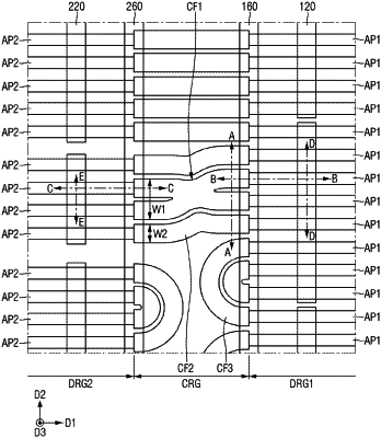
1. A semiconductor device comprising:
a substrate including a first region, a second region, and a connecting region placed between the first region and the second region;
a plurality of first multi-channel active patterns placed in the first region of the substrate;
a plurality of second multi-channel active patterns placed in the second region of the substrate;
a first connecting fin type pattern which is placed in the connecting region of the substrate and extends from the first region to the second region in a first direction; and
a field insulating film which is placed on the substrate and covers an upper surface of the first connecting fin type pattern,
wherein a width of the first connecting fin type pattern in a second direction decreases and then increases as it goes away from the first region, and
the first direction is perpendicular to the second direction.
|