| CPC H01L 27/11807 (2013.01) [H01L 21/823814 (2013.01); H01L 21/823878 (2013.01); H01L 27/0207 (2013.01); H01L 2027/11829 (2013.01); H01L 2027/11861 (2013.01); H01L 2027/11864 (2013.01); H01L 2027/11881 (2013.01)] | 12 Claims |

|
1. A method of manufacturing a semiconductor device, comprising:
forming a plurality of active fins extending in a first direction in a pair of cell areas on a substrate, the pair of cell areas being separated from each other by a power area;
forming a plurality of dummy gate structures, a plurality of gate spacers, and a plurality of gap fill patterns, each in a line shape extending in a second direction, substantially perpendicular to the first direction, such that each of the plurality of dummy gate structures and each of the plurality of gap fill patterns covers the plurality of active fins, alternately with respect to each other in the first direction;
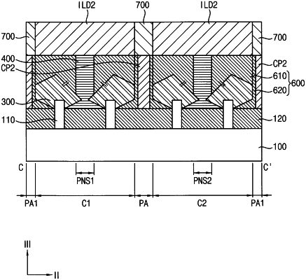
forming a cutting pattern in the power area in a line shape extending in the first direction such that the pair of cell areas are separated from each other;
removing the plurality of gap fill patterns; and
forming a junction layer in a gap space between neighboring dummy gate structures, of the plurality of dummy gate structures, such that the junction layer, for each set of neighboring dummy gate structures of the plurality of dummy gate structures, makes contact with the plurality of active fins in the pair of cell areas and the junction layer has a flat portion making contact with the cutting pattern.
|