| CPC H01L 27/11807 (2013.01) [H01L 2027/11831 (2013.01); H01L 2027/11851 (2013.01); H01L 2027/11875 (2013.01); H01L 2027/11881 (2013.01)] | 9 Claims |

|
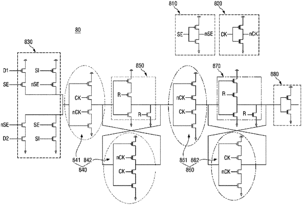
1. A vertical field effect transistor (VFET) cell implementing a scan flip-flop with a reset input comprising a plurality of circuits over 1st through 24th gate grids, which are consecutively formed and evenly spaced in the VFET cell,
wherein the 1st gate grid provides a one-fin scan inverter,
wherein the 2nd through 6th gate grids provide a scan stage circuit configured to receive a scan input signal, a data signal, a scan enable signal, and an inverted scan enable signal,
wherein the 7th through 11th gate grids provide a master latch,
wherein the 12th and 13th gate grids provide a two-fin clock inverter,
wherein the 14th gate grid provides an output circuit comprising a one-fin inverter,
wherein the 15th through 17th gate grids provide a slave data path circuit configured to receive a reset signal for the master latch,
wherein the 18th and 19th gate grids provide a master data path circuit configured to receive the reset signal for a slave latch, and
wherein the 20th through 24th gate grids provide the slave latch.
|