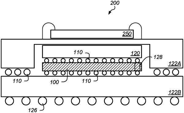
| CPC H01L 27/101 (2013.01) [H01G 4/228 (2013.01); H01L 23/13 (2013.01); H01L 23/481 (2013.01); H01L 23/49816 (2013.01); H01L 23/642 (2013.01); H01L 24/14 (2013.01); H01L 24/32 (2013.01); H01L 24/73 (2013.01); H01L 25/0657 (2013.01); H01L 25/16 (2013.01); H01L 25/18 (2013.01); H01L 28/40 (2013.01); H01L 23/49827 (2013.01); H01L 23/50 (2013.01); H01L 24/16 (2013.01); H01L 24/48 (2013.01); H01L 25/105 (2013.01); H01L 2224/0401 (2013.01); H01L 2224/13025 (2013.01); H01L 2224/1403 (2013.01); H01L 2224/14181 (2013.01); H01L 2224/16145 (2013.01); H01L 2224/16227 (2013.01); H01L 2224/16265 (2013.01); H01L 2224/32225 (2013.01); H01L 2224/45099 (2013.01); H01L 2224/48227 (2013.01); H01L 2224/73265 (2013.01); H01L 2225/06513 (2013.01); H01L 2225/06517 (2013.01); H01L 2225/1023 (2013.01); H01L 2225/1058 (2013.01); H01L 2225/1088 (2013.01); H01L 2924/00012 (2013.01); H01L 2924/00014 (2013.01); H01L 2924/1033 (2013.01); H01L 2924/12042 (2013.01); H01L 2924/1205 (2013.01); H01L 2924/1427 (2013.01); H01L 2924/1432 (2013.01); H01L 2924/1434 (2013.01); H01L 2924/1436 (2013.01); H01L 2924/15153 (2013.01); H01L 2924/15159 (2013.01); H01L 2924/15174 (2013.01); H01L 2924/15311 (2013.01); H01L 2924/15331 (2013.01); H01L 2924/157 (2013.01); H01L 2924/19011 (2013.01); H01L 2924/19041 (2013.01); H01L 2924/19042 (2013.01); H01L 2924/19103 (2013.01); H01L 2924/19104 (2013.01)] | 20 Claims |

|
1. A switched capacitor circuit, comprising:
a first semiconductor substrate;
a plurality of passive structures formed on the first semiconductor substrate, wherein the plurality of passive structures is arranged in a tiled pattern on the first semiconductor substrate, wherein a first passive structure in the plurality of passive structures includes at least a first capacitor formed on the first semiconductor substrate, and wherein a second passive structure in the plurality of passive structures includes at least a second capacitor formed on the first semiconductor substrate;
a second semiconductor substrate coupled to the first semiconductor substrate; and
one or more current consuming elements formed on the second semiconductor substrate;
wherein the first and second capacitors are coupled to a same current consuming element of the one or more current consuming elements, the first and second capacitors being coupled to the same current consuming element in a particular manner to provide a voltage conversion circuit for the same current consuming element.
|