| CPC H01L 27/0886 (2013.01) [H01L 23/50 (2013.01); H01L 23/5226 (2013.01); H01L 27/0688 (2013.01); H01L 29/6681 (2013.01); H01L 29/785 (2013.01)] | 10 Claims |

|
1. A semiconductor device, comprising:
logic cells and tap cells, which are two-dimensionally arranged on a substrate;
a first metal layer provided on the logic cells and the tap cells;
a second metal layer provided on the first metal layer; and
a power delivery network provided on a bottom surface of the substrate,
wherein a first logic cell, which is one of the logic cells, comprises:
a first active region and a second active region;
a gate electrode provided on the first active region and the second active region;
an active contact that is adjacent to the gate electrode; and
a gate contact electrically coupled to the gate electrode,
wherein a first tap cell, which is one of the tap cells and is adjacent to the first logic cell, comprises:
a first dummy region that is adjacent to the first active region; a second dummy region that is adjacent to the second active region;
a dummy electrode provided on the first dummy region and the second dummy region; and
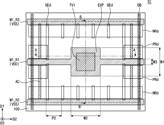
a through via which vertically extends from the power delivery network through the substrate,
wherein the first metal layer comprises a first power line and a second power line which extend across the first logic cell and the first tap cell in parallel to each other, and
wherein the power delivery network and the first power line are electrically connected to each other through the through via in the first tap cell.
|