| CPC H01L 27/0886 (2013.01) [H01L 29/42392 (2013.01); H01L 29/7851 (2013.01); H01L 29/78696 (2013.01)] | 28 Claims |

|
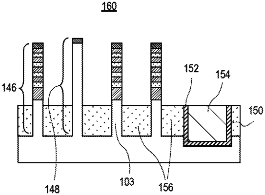
1. An integrated circuit structure, comprising:
a semiconductor island on a semiconductor substrate;
a first vertical arrangement of horizontal nanowires above a first fin protruding from the semiconductor substrate, a channel region of the first vertical arrangement of horizontal nanowires electrically isolated from the fin; and
a second vertical arrangement of horizontal nanowires above a second fin protruding from the semiconductor substrate, a channel region of the second vertical arrangement of horizontal nanowires electrically isolated from the second fin, wherein the semiconductor island is between the first vertical arrangement of horizontal nanowires and the second vertical arrangement of horizontal nanowires, and wherein the semiconductor island has an uppermost surface above an uppermost surface of the first vertical arrangement of horizontal nanowires and above an uppermost surface of the second vertical arrangement of horizontal nanowires.
|