| CPC H01L 27/088 (2013.01) [H01L 21/76224 (2013.01); H01L 21/823418 (2013.01); H01L 21/823481 (2013.01); H01L 29/40114 (2019.08); H01L 29/66825 (2013.01); H01L 29/7883 (2013.01); H10B 41/30 (2023.02); H01L 29/6656 (2013.01)] | 20 Claims |
|
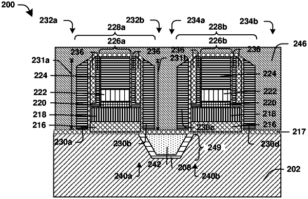
1. A semiconductor device, comprising:
a first fin defining a first active area;
a second fin defining a second active area;
a first implant region over a top surface of a first portion of the first fin and adjacent a sidewall of the first portion of the first fin;
a shallow trench isolation region between the first fin and the second fin, wherein the shallow trench isolation region covers a first portion of the first implant region adjacent the sidewall of the first portion of the first fin;
a second implant region over a second portion of the first implant region over the top surface of the first portion of the first fin;
a first gate structure over a second portion of the first fin; and
a second gate structure over a third portion of the first fin, wherein the first portion of the first fin is between the second portion of the first fin and the third portion of the first fin.
|