| CPC H01L 27/0727 (2013.01) [H01L 29/0696 (2013.01); H01L 29/7397 (2013.01); H01L 29/8611 (2013.01); H01L 29/7805 (2013.01); H01L 29/8613 (2013.01)] | 20 Claims |
|
1. A reverse conducting insulated gate power semiconductor device comprising a wafer having a first main side and a second main side opposite to the first main side, a first main electrode on the first main side and a second main electrode on the second main side, wherein the wafer comprises:
a first conductivity type base layer;
a second conductivity type collector layer in direct contact with the first conductivity type base layer to form a first pn junction, the second conductivity type collector layer in electrical contact with the second main electrode, wherein the second conductivity type is different from the first conductivity type;
a collector short electrically connecting the first conductivity type base layer to the second main electrode;
a pilot diode unit cell comprising:
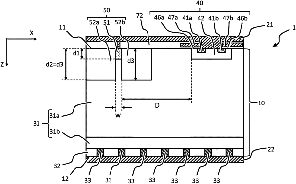
a second conductivity type anode region extending from the first main side to a first depth, wherein the anode region is in direct contact with the first main electrode and is in direct contact with the first conductivity type base layer to form a second pn junction and wherein a lateral size of the anode region in an orthogonal projection onto a vertical plane perpendicular to the first main side is equal to or less than 1 μm, a lateral direction being defined as a direction parallel to the first main side;
a first insulating layer arranged on a first lateral side surface of the anode region and extending from the first main side to a second depth that is greater than the first depth;
a second insulating layer arranged on a second lateral side surface of the anode region and extending from the first main side to a third depth that is greater than the first depth, the second insulating layer being laterally spaced from the first insulating layer by the anode region, wherein, in a vertical cross-section of the pilot diode unit cell with the vertical plane, a distance between the first insulating layer and the second insulating layer is equal to or less than 1 μm; and
a plurality of active unit cells adjacent to the first main side wherein each active unit cell comprises:
a first conductivity type first source layer in electrical contact with the first main electrode on the first main side;
a second conductivity type base layer on a side of the first conductivity type base layer opposite to the collector layer, wherein the first conductivity type base layer is in direct contact with the second conductivity type base layer to form a third pn junction and wherein the second conductivity type base layer is in direct contact with the first source layer to form a fourth pn junction; and
a first gate electrode, which is separated from the first source layer, the second conductivity type base layer and the first conductivity type base layer by a first gate insulating layer to form a field effect transistor structure.
|