| CPC H01L 27/0664 (2013.01) [H01L 21/765 (2013.01); H01L 29/1095 (2013.01); H01L 29/407 (2013.01); H01L 29/66136 (2013.01); H01L 29/66348 (2013.01); H01L 29/7397 (2013.01); H01L 29/8613 (2013.01)] | 7 Claims |
|
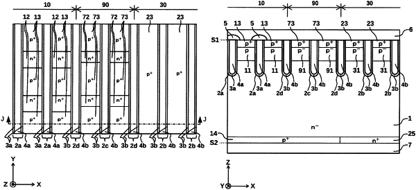
1. A semiconductor device comprising:
a semiconductor substrate including a drift layer of a first conductivity type between a first main surface and a second main surface facing the first main surface;
a hole injection region including:
a hole injection layer of a second conductivity type provided in a surface layer on the first main surface side of the semiconductor substrate, and
a semiconductor layer of the second conductivity type provided in a surface layer on the second main surface side;
a diode region including:
an anode layer of the second conductivity type provided in the surface layer on the first main surface side of the semiconductor substrate,
an anode contact layer of the second conductivity type selectively provided in the surface layer on the first main surface side of the anode layer, the anode contact layer having a higher impurity concentration than the anode layer, and
a cathode layer of the first conductivity type provided in the surface layer on the second main surface side of the semiconductor substrate,
the diode region having no semiconductor layer of the first conductivity type between the second main surface side of the anode layer and the first main surface, and
the hole injection region and the diode region being not directly arranged adjacent to each other;
a boundary region including:
a boundary portion semiconductor layer of the second conductivity type provided between the diode region and the hole injection region, the boundary portion semiconductor layer provided in the surface layer on the first main surface side of the semiconductor substrate,
a carrier injection suppression layer of the first conductivity type provided in a surface layer of the boundary portion semiconductor layer and extending to the first main surface,
a boundary portion contact layer of the second conductivity type provided in the surface layer of the boundary portion semiconductor layer, the boundary portion contact layer having a higher impurity concentration than the boundary portion semiconductor layer,
an electrode on and connected to the carrier injection suppression layer and the boundary portion contact layer, and
the semiconductor layer of the second conductivity type provided in the surface layer on the second main surface side is provided to protrude from the hole injection region in the surface layer on the second main surface side of the semiconductor substrate; and
a boundary dummy gate electrode provided on the first main surface side of the semiconductor substrate between the diode region and the boundary region, the boundary dummy gate electrode facing the boundary portion semiconductor layer and the drift layer via a gate insulating film, the boundary dummy gate electrode to which no gate driving voltage is applied.
|