| CPC H01L 25/18 (2013.01) [H01L 23/3128 (2013.01); H01L 23/481 (2013.01); H01L 23/49811 (2013.01); H01L 23/49822 (2013.01); H01L 23/5226 (2013.01); H01L 23/5389 (2013.01); H01L 23/66 (2013.01); H01L 24/20 (2013.01); H01L 24/16 (2013.01); H01L 2223/6677 (2013.01); H01L 2224/16227 (2013.01)] | 20 Claims |
|
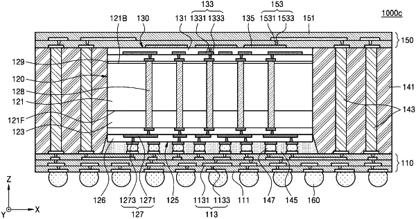
1. A semiconductor package comprising:
a first substrate comprising a first conductive pattern;
a first semiconductor chip on the first substrate; and
an upper structure on the first semiconductor chip such that the first semiconductor chip is between the upper structure and the first substrate, the upper structure including an insulating layer and a second conductive pattern in the insulating layer,
wherein the first semiconductor chip comprises
a semiconductor substrate,
a first back end of line (BEOL) structure on a first surface of the semiconductor substrate, the first BEOL structure comprising a first interconnect pattern, and
a second BEOL structure on a second surface of the semiconductor substrate, the second BEOL structure comprising a second interconnect pattern and a first antenna pattern configured to transmit and receive a radio signal, and
the second conductive pattern is electrically connected to the first antenna pattern.
|