| CPC H01L 25/18 (2013.01) [H01L 25/071 (2013.01); H01L 25/50 (2013.01); H01L 23/24 (2013.01); H01L 24/32 (2013.01); H01L 24/33 (2013.01); H01L 2224/32245 (2013.01); H01L 2224/33181 (2013.01); H01L 2924/10272 (2013.01); H01L 2924/1033 (2013.01); H01L 2924/1203 (2013.01); H01L 2924/13055 (2013.01); H01L 2924/15747 (2013.01)] | 18 Claims |
|
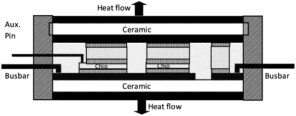
1. A semiconductor device sub-assembly comprising:
at least two power semiconductor devices; and
a contact of a first type, wherein a first power semiconductor device is located on a first side of the contact of a first type, and wherein a second power semiconductor device is located on a second side of the contact of a first type, wherein the second side is opposite to the first side;
at least two contacts of a second type, wherein one of the contacts of a second type is connected to a top side of the first power semiconductor device and another of the contacts of a second type is connected to a bottom side of the second power semiconductor device; and
a spacer, wherein the contacts of a second type are electrically connected to each other using the spacer.
|