| CPC H01L 25/0753 (2013.01) [H01L 33/50 (2013.01); H01L 33/58 (2013.01); H01L 33/62 (2013.01)] | 20 Claims |
|
1. A light-emitting diode micro display device, comprising:
a circuit substrate having a plurality of conductive patterns;
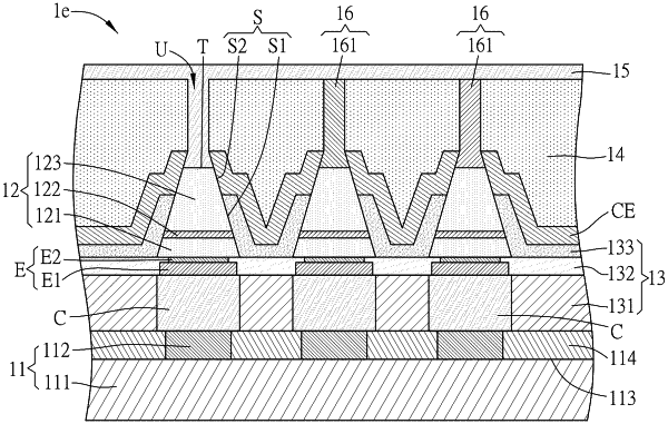
a plurality of micro light-emitting elements bonded to the circuit substrate and disposed corresponding to the conductive patterns, wherein each of the micro light-emitting elements has a bottom surface, a top surface and a side wall connected to the bottom surface and the top surface, the bottom surface connects to the corresponding conductive pattern, the side wall has a first sidewall portion and a second sidewall portion connected to the first sidewall portion, and the first sidewall portion is disposed adjacent to the circuit substrate, while the second sidewall portion is disposed away from the circuit substrate;
an insulating layer disposed on the circuit substrate, covering the first sidewall portions and exposing the second sidewall portions;
a common electrode layer disposed on the circuit substrate and covering the insulating layer and the second sidewall portions of the plurality of micro light-emitting elements, wherein the common electrode layer is electrically connected to the micro light-emitting elements;
a planarization layer disposed on the common electrode layer, wherein the planarization layer, the common electrode layer, and the top surfaces of the micro light-emitting elements together define a plurality of recesses;
a light conversion layer disposed in at least a part of the recesses; and
a protection layer disposed on and completely covering the planarization layer and the light conversion layer,
wherein, the common electrode layer contacts the second sidewall portions and exposes the top surface of each of the micro light-emitting elements.
|