| CPC H01L 25/072 (2013.01) [H01L 23/3735 (2013.01); H01L 23/5385 (2013.01); H01L 23/5386 (2013.01); H01L 24/32 (2013.01); H01L 24/49 (2013.01); H01L 2224/48091 (2013.01); H01L 2224/49111 (2013.01); H01L 2224/73265 (2013.01); H01L 2924/19107 (2013.01)] | 19 Claims |

|
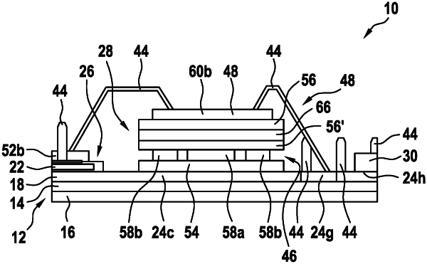
1. A power semiconductor module, comprising:
a main substrate with a main conductive layer separated into conductive areas;
a plurality of power semiconductor chips, wherein each power semiconductor chip has a first power electrode, a second power electrode, and a gate electrode, wherein each power semiconductor chip is bonded to the main conductive layer with the first power electrode and wherein a first group of the power semiconductor chips is connected in parallel via the second power electrodes and a second group of the power semiconductor chips is connected in parallel via the second power electrodes;
a first insulation layer attached to the main conductive layer;
a first conductive layer provided on the first insulation layer, wherein the first conductive layer provides a first gate conductor area electrically connected to the gate electrodes of the first group and a first auxiliary emitter conductor area electrically connected to power electrodes of the first group;
a second insulation layer attached to the first conductive layer; and
a second conductive layer provided on the second insulation layer, wherein the second conductive layer provides a second gate conductor area electrically connected to the gate electrodes of the second group and a second auxiliary emitter conductor area electrically connected to power electrodes of the second group;
wherein the main conductive layer, the first insulation layer, the first conductive layer, the second insulation layer and the second conductive layer are stacked with respect to each other.
|