| CPC H01L 25/0657 (2013.01) [H01L 23/5226 (2013.01); H01L 23/5286 (2013.01); H01L 24/13 (2013.01); H01L 25/50 (2013.01)] | 20 Claims |
|
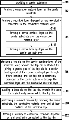
1. A stacked die structure, comprising:
a base die comprising:
a base semiconductor substrate;
a base interconnection layer disposed on the base semiconductor substrate; and
a base bonding layer disposed on and electrically connected to the base interconnection layer;
a top die stacked on the base die and electrically connected to the base die, wherein the top die comprises:
a top bonding layer hybrid bonded to the base bonding layer of the base die;
a top semiconductor substrate disposed on the top bonding layer;
a top interconnection layer disposed on the top semiconductor substrate, wherein the top interconnection layer comprises a dielectric layer, a plurality of conductive layers embedded in the dielectric layer, and a plurality of conductive vias joining the plurality of conductive layers; and
top conductive pads and top grounding vias embedded in the dielectric layer and disposed on the plurality of conductive layers; and
a plurality of conductive terminals electrically connected to the top die.
|