| CPC H01L 25/0657 (2013.01) [H01L 25/167 (2013.01); H01L 33/005 (2013.01); H01L 33/44 (2013.01); H01L 33/62 (2013.01); H01L 2933/0066 (2013.01)] | 20 Claims |
|
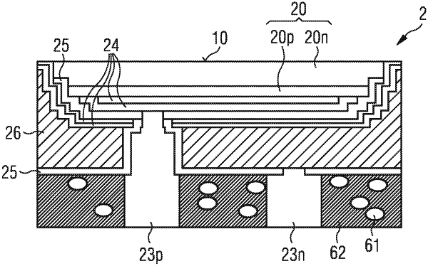
1. An optoelectronic semiconductor device which is surface-mountable, comprising:
at least one semiconductor chip which emits light during operation and comprises electrical contact pads,
an opaque base body laterally surrounding the at least one semiconductor chip so that side surfaces of the semiconductor chip are directly covered by the base body all around,
at least one electrical fanning layer with electrical conductor tracks, and
electrical connection pads for external electrical contacting of the semiconductor device,
wherein
the contact pads and the connection pads are located on different sides of the fanning layer,
the contact pads are electrically connected to the associated connection pads by means of the fanning layer,
the connection pads are expanded relative to the contact pads,
the base body extends between the semiconductor chip and the fanning layer and/or the contact pads are embedded in a chip potting of the semiconductor chip and the contact pads terminate flush with the chip potting, and
the at least one semiconductor chip is a laser diode, a superluminescent diode, or a light emitting diode and configured to emit the light in an infrared range, a visible range, or an ultraviolet range.
|