| CPC H01L 24/14 (2013.01) [H01L 21/76802 (2013.01); H01L 21/76877 (2013.01); H01L 23/488 (2013.01); H01L 2224/0401 (2013.01); H01L 2224/13 (2013.01)] | 20 Claims |
|
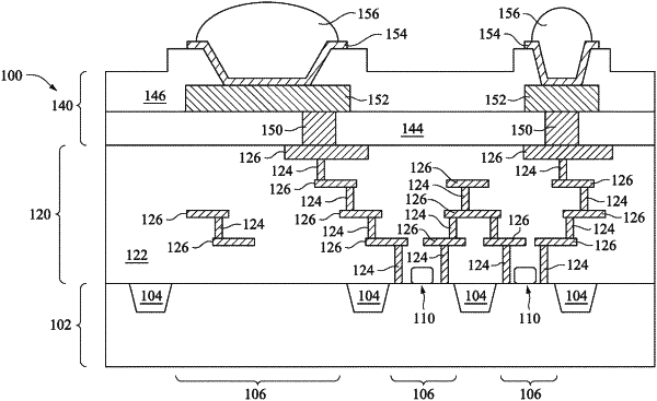
1. A semiconductor device structure, comprising:
a bonding pad disposed over a substrate;
a first conductive feature disposed adjacent the bonding pad, wherein a center portion of the bonding pad and the first conductive feature are a first distance apart, an edge portion of the bonding pad and the first conductive feature are a second distance apart, and the first distance is smaller than the second distance; and
a passivation layer disposed over the bonding pad and the first conductive feature, wherein the passivation layer comprises:
a first passivation sublayer comprising a first dielectric material;
a second passivation sublayer disposed over the first passivation sublayer, the second passivation sublayer comprising a second dielectric material different from the first dielectric material; and
a third passivation sublayer disposed over the second passivation sublayer.
|