| CPC H01L 24/14 (2013.01) [H01L 23/14 (2013.01); H01L 23/49811 (2013.01); H01L 23/5384 (2013.01); H01L 23/5385 (2013.01); H01L 23/5386 (2013.01)] | 19 Claims |
|
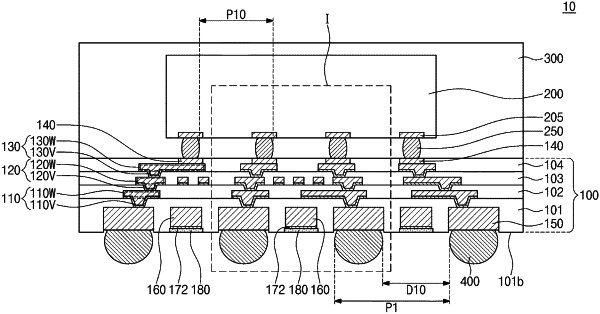
1. A semiconductor package comprising:
a redistribution substrate; and
a semiconductor chip disposed on a top surface of the redistribution substrate,
wherein the redistribution substrate comprises:
under bump patterns laterally spaced apart from each other;
a dummy pattern disposed between the under bump patterns;
a passivation pattern disposed on a bottom surface of the dummy pattern;
an insulating layer covering top surfaces and sidewalls of the under bump patterns, directly contacting a sidewall and a top surface of the dummy pattern, and directly contacting a sidewall of the passivation pattern; and
a redistribution pattern disposed on one of the under bump patterns and electrically connected to the one under bump pattern,
wherein the passivation pattern includes a different material from that of the insulating layer, and
wherein bottom surfaces of the under bump patterns are disposed at a higher level than a bottom surface of the passivation pattern.
|