| CPC H01L 23/66 (2013.01) [H01L 23/3114 (2013.01); H01L 23/49861 (2013.01)] | 20 Claims |
|
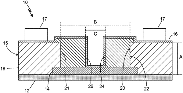
1. An integrated circuit device comprising:
a wafer; and
an interconnect layer at least partially covering the wafer, the interconnect layer comprising:
a low radio frequency (RF) loss primary coating that forms a main portion of the interconnect layer;
a trench formed in and extending through a full thickness of the primary coating to expose a feature that is positioned on the wafer;
a high aspect ratio patternable secondary coating within the trench; and
a via formed in the secondary coating, wherein an aspect ratio of the via is greater than an aspect ratio of the trench.
|