| CPC H01L 23/552 (2013.01) [H01L 21/50 (2013.01); H05K 9/0026 (2013.01)] | 20 Claims |

|
1. A method for fabricating an electronic assembly, the method comprising:
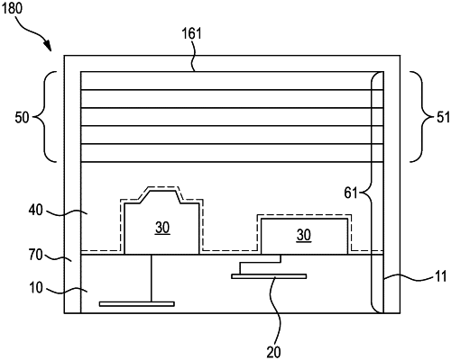
providing a board comprising a plurality of traces having an electrical conductivity, and at least two spatially spaced semiconductor integrated circuits which are mounted on a first main surface of the board and are electrically connected with the plurality of traces;
disposing a protection layer on the at least two spatially spaced integrated circuits;
forming a multilayer article by disposing a magnetic field shielding film on a main top surface of the protection layer, the magnetic field shielding film being a multilayer film comprising a magnetic field shielding layer disposed between first and second adhesive layers, each of the first and second adhesive layers being configured to bond the magnetic field shielding layer to a layer adjacent to the magnetic field shielding layer;
producing at least two cut multilayer articles by cutting the multilayer article along a thickness direction of the multilayer article at a predetermined cutting point between the at least two spatially spaced integrated circuits, each of the cut multilayer articles comprising a cut multilayer edge surface comprising exposed edges of the board, the protection layer, and the magnetic field shielding film at the predetermined cutting point; and
with respect to at least one of the cut multilayer articles, fabricating the electronic assembly by disposing a first metal layer at least on a main top surface and the cut multilayer edge surface of the at least one cut multilayer article.
|