| CPC H01L 23/552 (2013.01) [H01L 21/50 (2013.01); H01L 23/528 (2013.01)] | 15 Claims |
|
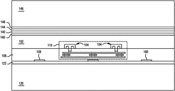
1. An integrated circuit (IC) structure comprising:
a semiconductor substrate having a circuit disposed on a front side of the semiconductor substrate;
a diffusion barrier layer disposed on a backside of the semiconductor substrate;
an electromagnetic radiation blocking layer disposed on the diffusion barrier layer and on the backside of the semiconductor substrate opposite from the front side of the semiconductor substrate, wherein the electromagnetic radiation blocking layer is a blanket layer covering an entirety of the backside of the semiconductor substrate; and
a support substrate bonded to the semiconductor substrate, the electromagnetic radiation blocking layer being disposed between the semiconductor substrate and the support substrate.
|