| CPC H01L 23/544 (2013.01) [H01L 23/481 (2013.01); H01L 24/83 (2013.01); H01L 2223/54426 (2013.01); H01L 2224/8313 (2013.01)] | 9 Claims |
|
1. A method of manufacturing a semiconductor architecture, the method including:
providing a first wafer comprising a carrier substrate;
providing a stopper layer on the carrier substrate;
providing a sacrificial layer on the stopper layer;
providing alignment marks in the carrier substrate from a first surface of the carrier substrate to a first surface of the stopper layer;
providing a first semiconductor device on the first surface of the carrier substrate based on locations of the alignment marks provided on the first surface of the carrier substrate;
removing the sacrificial layer;
removing the stopper layer; and
providing a second semiconductor device on a second surface of the carrier substrate based on locations of the alignment marks provided on the second surface of the carrier substrate,
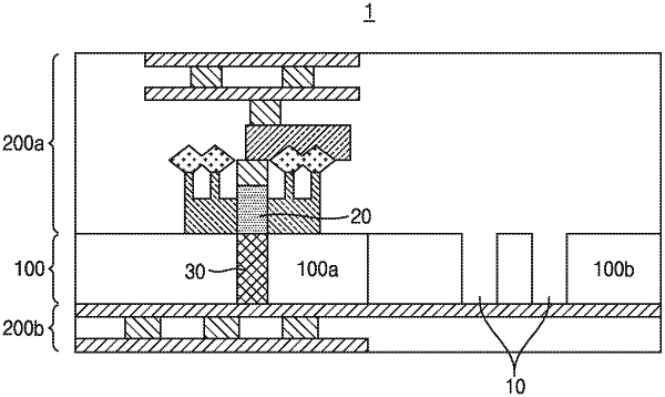
wherein providing the second semiconductor device further comprises providing a through silicon via (TSV) based on the locations of the alignment marks such that the through silicon via is aligned with a buried power rail (BPR) included in the first semiconductor device.
|