| CPC H01L 23/53276 (2013.01) [H01L 21/76805 (2013.01); H01L 21/76877 (2013.01); H01L 23/5226 (2013.01); H01L 23/53257 (2013.01); H01L 23/53271 (2013.01); H01L 23/5328 (2013.01)] | 20 Claims |
|
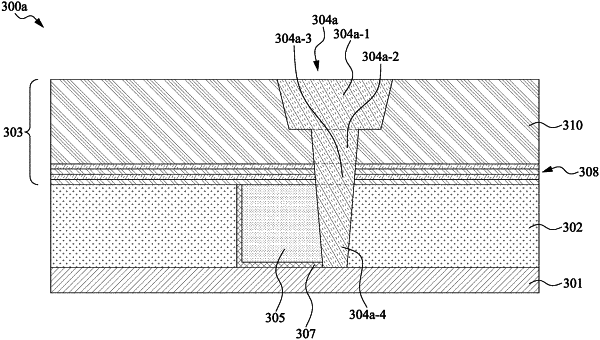
1. A semiconductor structure, comprising:
a plurality of two-dimensional (2D) conductive structures;
an isolation structure separating the 2D conductive structures;
a dielectric structure longitudinally stacked on the 2D conductive structures and the isolation structure; and
at least one interconnect structure disposed in the dielectric structure and extending along an interface between one of the 2D conductive structures and the isolation structure, so that the interconnect structure partially contacts the one of the 2D conductive structures and partially contacts the isolation structure,
wherein the interconnect structure includes a bottom part disposed between the one of the 2D conductive structures and the isolation structure,
wherein a top of each of the 2D conductive structures and a top of the isolation structure are coplanar, and
wherein the bottom part of the interconnect structure has a tapered vertical cross sectional shape.
|