| CPC H01L 23/5286 (2013.01) [H01L 23/481 (2013.01); H01L 27/092 (2013.01); H01L 27/0924 (2013.01)] | 17 Claims |

|
1. A semiconductor device including a standard cell region, the semiconductor device comprising:
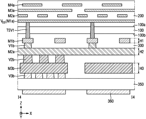
a substrate including a first surface and a second surface, which are opposite to each other;
a first power wiring, which extends in a first direction on the first surface of the substrate, and is configured to provide a first power voltage to the standard cell region;
a second power wiring, which extends in the first direction on the first surface of the substrate, is arranged alternately with the first power wiring in a second direction intersecting the first direction, and is configured to provide a second power voltage different from the first power voltage to the standard cell region;
a first back routing wiring on the second surface of the substrate;
a plurality of first tab cell regions arranged along the second direction; and
a plurality of second tab cell regions, which are spaced apart from the plurality of first tab cell regions and are arranged along the second direction,
wherein each of the first tab cell regions includes a first through via, which penetrates the substrate and connects the first power wiring and the first back routing wiring, and
wherein each of the second tab cell regions includes a second through via, which penetrates the substrate and connects the second power wiring and the first back routing wiring.
|