| CPC H01L 23/5283 (2013.01) [H01L 21/311 (2013.01); H01L 21/76816 (2013.01); H01L 21/76877 (2013.01); H01L 21/76895 (2013.01); H01L 23/5226 (2013.01); H01L 23/535 (2013.01); H10B 41/10 (2023.02); H10B 41/27 (2023.02); H10B 43/10 (2023.02); H10B 43/27 (2023.02); H10B 43/40 (2023.02); H10B 43/50 (2023.02)] | 16 Claims |

|
1. A semiconductor device, comprising:
a stack of word line layers and insulating layers that are stacked alternatingly; and
channel structures formed in a first array region and a second array region of the stack, the first array region and the second array region being positioned at opposing sides of the stack, wherein
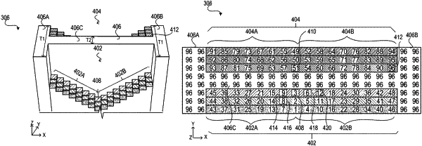
a first staircase is formed between the first array region and the second array region,
a second staircase is formed between the first array region and the second array region,
a portion of the stack is positioned between the first staircase and the second staircase and between the first array region and the second array region,
the first staircase has first stairs with a first step-down direction and second stairs with a second step-down direction, the first step-down direction being opposite to the second step-down direction, and
each of all of the first stairs and each of all of the second stairs corresponds to a different one of the word line layers.
|