| CPC H01L 23/5283 (2013.01) [H01L 21/76816 (2013.01); H01L 21/76877 (2013.01); H01L 23/5226 (2013.01); H10B 41/27 (2023.02); H10B 43/27 (2023.02)] | 12 Claims |
|
1. A three-dimensional memory device, comprising:
an alternating stack of insulating layers and electrically conductive layers;
memory stack structures vertically extending through the alternating stack, wherein each of the memory stack structures comprises a vertical semiconductor channel and a vertical stack of memory elements located at levels of the electrically conductive layers;
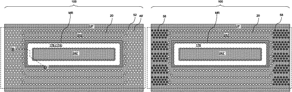
a perforated dielectric moat structure comprising a dielectric fill material vertically extending through the alternating stack and including a plurality of lateral openings at each level of the insulating layers and not including any opening at levels of the electrically conductive layers; and
an interconnection via structure laterally surrounded by the perforated dielectric moat structure and vertically extending through each insulating layer within the alternating stack and contacting a top surface of an underlying metal interconnect structure;
wherein: the perforated dielectric moat structure comprises, at each level of the insulating layers, two rows of lengthwise dielectric pillar portions laterally extending along a first horizontal direction and two columns of widthwise dielectric pillar portions extending along a second horizontal directions that is perpendicular to the first horizontal direction;
each row of lengthwise dielectric pillar portions comprises three or more lengthwise dielectric pillar portions which have a first center-to-center pitch;
each column of widthwise dielectric pillar portions comprises two or more widthwise dielectric pillar portions which have a second center-to-center pitch; and
a ratio of the second center-to-center pitch to the first center-to-center pitch is in a range from 1.50 to 2.0;
wherein the memory stack structures are arranged in a hexagonal array having a nearest-neighbor center-to-center pitch that is the same as the first center-to-center pitch;
wherein: the hexagonal array comprises a regular hexagonal array; and
the regular hexagonal array has the nearest-neighbor center-to-center pitch along the first horizontal direction, along a horizontal direction that is azimuthally offset from the first horizontal direction by 60 degrees, and along a horizontal direction that is azimuthally offset from the first horizontal direction by 120 degrees.
|