| CPC H01L 23/5226 (2013.01) [H01L 21/76805 (2013.01); H01L 21/76807 (2013.01); H01L 23/53238 (2013.01); H01L 23/5329 (2013.01); H01L 23/53295 (2013.01); H01L 21/76834 (2013.01); H01L 21/76849 (2013.01); H01L 2924/0002 (2013.01)] | 20 Claims |
|
1. A device comprising:
a first dielectric layer having a top surface extending to a first height;
a copper-comprising feature disposed within the first dielectric layer;
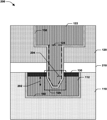
a cobalt-comprising cap feature disposed on the copper-comprising feature, the cobalt-comprising cap feature having a first sidewall and an opposing second sidewall and a top surface extending from the first sidewall to the second sidewall, wherein the top surface of the cobalt-comprising cap feature extends to the first height, and further wherein the cobalt-comprising cap feature further includes tungsten and phosphorous;
an etch stop layer disposed directly on the top surface of the cobalt-comprising cap feature and the top surface of the first dielectric layer;
a barrier feature at least partially surrounding the copper-comprising feature and physically contacting the first sidewall and the second sidewall of the cobalt-comprising cap feature; and
a copper-comprising via extending through the cobalt-comprising cap feature and into the copper-comprising feature, wherein the copper-comprising via includes a tapered portion disposed within the copper-comprising feature, the tapered portion including a first tapered sidewall edge on a first side of the tapered portion, a second tapered sidewall edge on a second side of the tapered portion that is opposite the first side, and a bottommost edge extending from a first interface with the first tapered sidewall edge to a second interface with the second tapered sidewall edge, wherein the first interface is spaced apart from the second interface and the bottommost edge is substantially parallel to the top surface of the first dielectric layer.
|