| CPC H01L 23/3736 (2013.01) [C23C 14/165 (2013.01); C23C 18/38 (2013.01); C25D 3/38 (2013.01); C25D 3/46 (2013.01); H01L 21/2855 (2013.01); H01L 21/288 (2013.01); H01L 21/76873 (2013.01); H01L 21/78 (2013.01)] | 11 Claims |
|
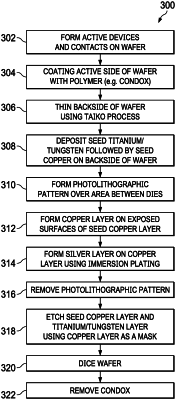
1. A process for making a semiconductor device, comprising:
forming a first diffusion barrier layer on an active side of a semiconductor wafer;
forming a second diffusion barrier layer on a backside of the semiconductor wafer;
forming a first seed copper layer on the first diffusion barrier layer;
forming a second seed copper layer on the second diffusion barrier layer;
forming a first copper layer on the first seed copper layer;
forming a second copper layer on the second seed copper layer; and
immersion plating a silver layer on the second copper layer.
|