| CPC H01L 23/3735 (2013.01) [H01L 23/3736 (2013.01); H05K 1/0204 (2013.01); H05K 1/0271 (2013.01); H05K 7/205 (2013.01); H05K 7/20509 (2013.01); H05K 2201/068 (2013.01); H05K 2201/09136 (2013.01)] | 8 Claims |
|
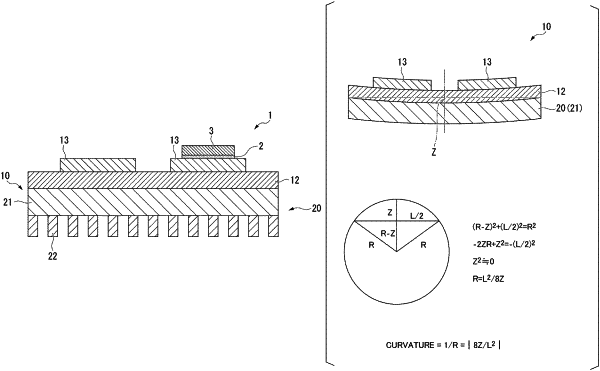
1. A heat sink integrated insulating circuit substrate comprising:
a heat sink including a top plate part and a cooling fin;
an insulating resin layer formed on the top plate part of the heat sink; and
a circuit layer made of metal pieces arranged in a circuit pattern on a surface of the insulating resin layer opposite to the heat sink,
wherein, when a maximum length of the top plate part of the heat sink is defined as L, an amount of warpage of the top plate part of the heat sink is defined as Z, and deformation of protruding toward a bonding surface side between the top plate part of the heat sink and the insulating resin layer is defined as a positive amount of warpage, and a curvature of the heat sink is defined as C=|(8×Z)/L2|,
a ratio P/Cmax between a maximum curvature Cmax (1/m) of the heat sink during heating from 25° C. to 300° C. and peel strength P (N/cm) of the insulating resin layer satisfies P/Cmax>60.
|