| CPC H01L 23/3733 (2013.01) [H01L 21/481 (2013.01); H01L 21/4871 (2013.01); H01L 23/16 (2013.01); H01L 23/3121 (2013.01); H01L 23/367 (2013.01); H01L 23/4334 (2013.01); H01L 23/49562 (2013.01); H01L 24/32 (2013.01); H01L 24/73 (2013.01); H01L 24/84 (2013.01); H01L 2924/181 (2013.01); H02P 27/08 (2013.01)] | 17 Claims |
|
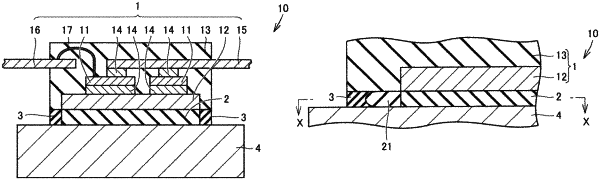
1. A semiconductor device comprising:
a semiconductor module;
an insulating resin layer bonded to the semiconductor module and containing a first resin;
a frame member disposed to surround the insulating resin layer and including a porous material; and
a heat sink sandwiching the insulating resin layer and the frame member between the semiconductor module and the heat sink, wherein
the frame member is compressed in a state of being sandwiched between the semiconductor module and the heat sink,
the insulating resin layer is filled in a region surrounded by the semiconductor module, the heat sink, and the frame member, and
the first resin enters a pore of the porous material.
|