| CPC H01L 22/12 (2013.01) [G01N 21/9505 (2013.01)] | 20 Claims |
|
1. A method of qualifying semiconductor wafer processing, said method comprising:
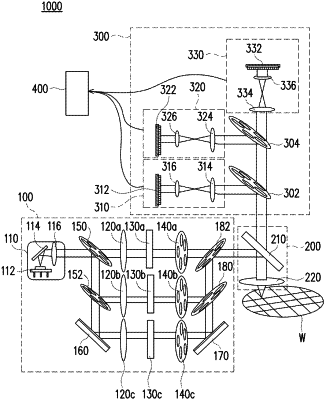
using a common light source, emitting light having wavelengths in both a first waveband and a second waveband;
separating the light emitted using the common light source according to waveband using dividing optics, such that the light emitted using the common light source in the first waveband is directed along a first optical path, while the light emitted using the common light source in the second waveband is directed along a second optical path;
regulating a first optical parameter of the common source light in the first waveband using a first optical element arranged along the first optical path;
regulating a second optical parameter of the common source light in the second waveband using a second optical element arranged along the second optical path;
combining the source light in the first waveband after it passes through the first optical element with the source light in the second waveband after it passes through the second optical element using combining optics to produce combined source light;
illuminating a semiconductor wafer with the combined source light;
separating light reflected from the semiconductor wafer as a result of said illuminating, said separating dividing the reflected light according to waveband;
generating a first image of the semiconductor wafer based on reflected light separated into the first waveband;
generating a second image of the semiconductor wafer base on reflected light separated into the second waveband; and,
analyzing the first and second images to qualify the semiconductor wafer based on a predetermined value of a defect count;
wherein the analyzing includes applying a first imaging processing to the first image to detect a first type of defect in the semiconductor wafer and applying a second imaging processing to the second image to detect a second type of defect in the semiconductor wafer, wherein the first type of defect and the second type of defect are different types of defects.
|